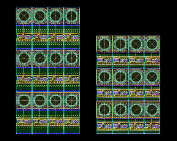
X-FAB Silicon Foundries has released an isolation class within its 180nm XH018 semiconductor process. Designed to support more compact and efficient single-photon avalanche diode (SPAD) implementations, this new isolation class enables tighter functional integration, improved pixel density and higher fill factor – resulting in a smaller chip area.
SPADs are critical components in a wide range of emerging applications, including lidar for autonomous vehicles and 3D imaging and depth sensing in AR/VR systems.
To enable high-resolution SPAD arrays, a compact pitch and elevated fill factor are essential. The new ISOMOS1, a 25V isolation class module, enables significantly more compact transistor isolation structures, eliminating the need for an additional mask layer and aligning perfectly with X-FAB’s other SPAD variants.
The benefits of this update are clear when comparing SPAD pixel layouts, says X-FAB. In a typical 4 x 3 SPAD array with 10 x 10µm² optical areas, the adoption of the new isolation class enables a 25% reduction in total area and boosts fill factor by 30% compared to the previously available isolation class. With optimized pixel design, F-FAB says that even greater gains in area efficiency and detection sensitivity are achievable.
The advancement is designed to benefit applications in which high-resolution sensing with a compact footprint is essential. It enables accurate depth sensing in multiple scenarios, including industrial distance detection and robotics sensing, for example, by protecting the area around a robot and avoiding collisions when robots are working as cobots. The isolation class also aims to open up opportunities for a broader range of SPAD-based systems requiring low-noise, high-speed single-photon detection within a compact footprint.
Heming Wei, X-FAB’s technical marketing manager for Optoelectronics, explained, “The introduction of a new isolation class in XH018 marks an important step forward for SPAD integration. It enables tighter layouts and better performance, while allowing for more advanced sensing systems to be developed using our proven, reliable 180nm platform.”


